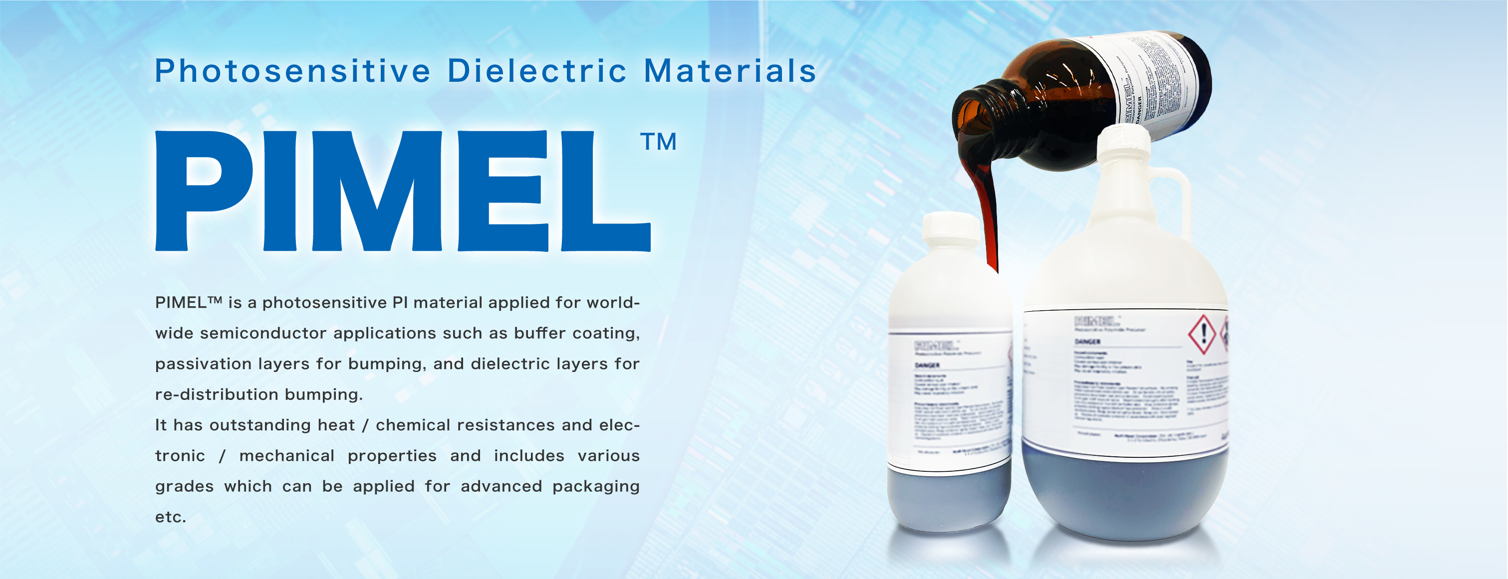
PIMEL™ is a photosensitive PI material that is used worldwide for semiconductor applications such as buffer coatings, passivation layers for bumping, and dielectric layers for re-distribution bumping.
It has outstanding heat / chemical resistance and electronic / mechanical properties, and is available in various grades that can be used for purposes such as advanced packaging.
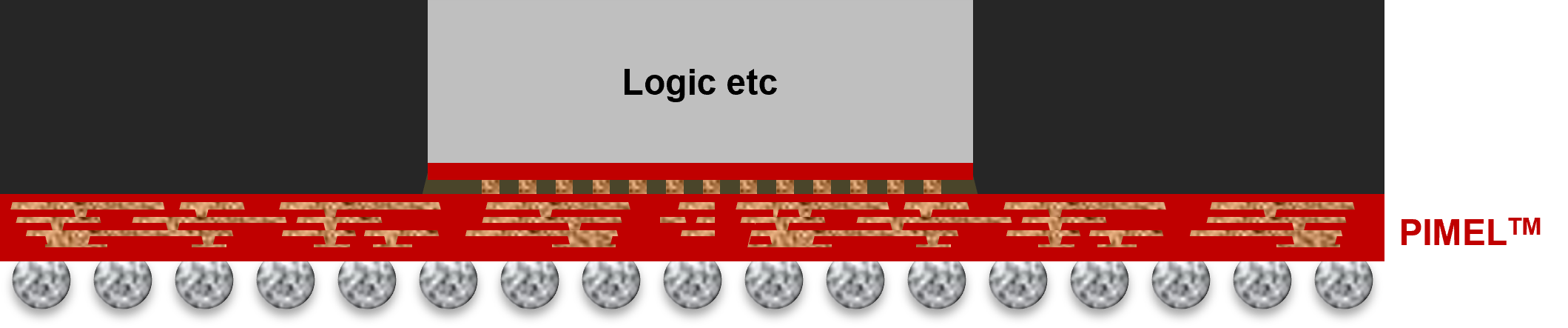
Our products are mainly used in semiconductor applications, for advanced packages that require multiple -layers or other specific functions.
Conventional packages
We have many years of mass- production experience in conventional packages for the semiconductor market.
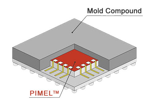
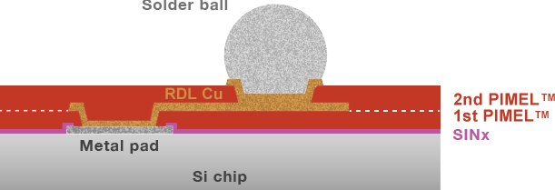
Buffer Coating
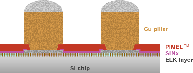
Flip Chip(Cu pillar)
WLCSP
Fan-Out(Single Die)
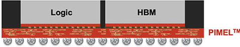
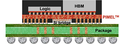
Advanced packages
We are expanding our sales of advanced packages that require cutting-edge technology.
Fan-out(Heterogeneous)
Fan-out(Heterogeneous with Si Bridge)
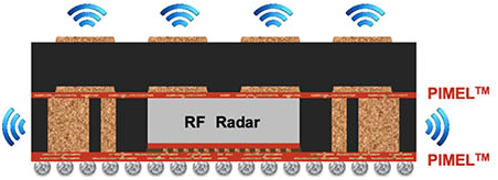
Fan-out(AiP)
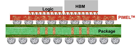
RDL Interposer
Our products are photosensitive and can be finely patterned on a micrometer scale. They can be coated not only on wafers but also on panels and other substrates.
We have a diverse product lineup to meet a wide range of applications and requirements. For detailed information, please send an inquiry using the form below.
BL-series
BM-series
AM-series
MA-series
LV-series
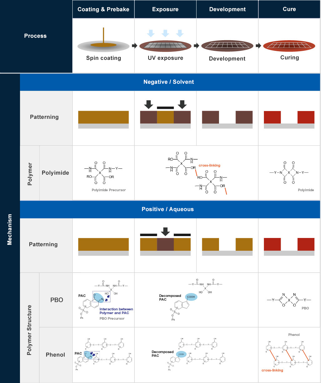
Development
Solvent
Solvent
Aqueous
Aqueous
Solvent
Patterning
Negative
Negative
Positive
Positive
Negative
Structure
Polyimide
Polyimide
PBO
Phenolic Resin
Polyimide
Application examples
WLCSP,Fan-Out
RDL+WB,Flip Chip
Buffer Coating
Buffer Coating
Panel
Features
Wide cure margin
(200~390 degC)
High elongation
Compatibility with Cu
Wide cure margin
(200~390 degC)
High Tg&Young’s modulus
Compatibility with Cu
High sensitivity
Low curing temperature
(200~390 degC)
Low stress
Compatibility with slit coating
Wide cure margin
(200~390 degC)
High elongation
Compatibility with Cu
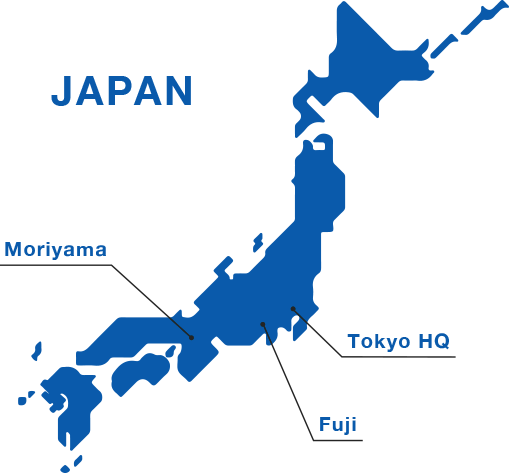
We have three offices in Japan, and also distributors and affiliates in other countries.