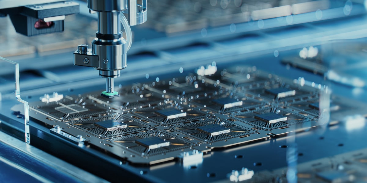
SUNFORT™'s Capabilities Pioneering the Future of Fine Pattern
The technology that supports the performance of next-generation devices is SUNFORT™'s high resolution and adhesion. It elevates the quality of substrate circuit manufacturing to a higher level.
Achieving High Resolution and High Adhesion Required for Fine Pattern Formation
SUNFORT™ achieves the high resolution and high adhesion required for fine pattern formation. It is highly regarded in the industry for the following features.
-
Expanding Possibilities Through Improved ResolutionFine wiring with L/S=2/2 µm or less can be formed. This enables the miniaturization and high density of high-performance devices such as smartphones and AI equipment.
-
High AdhesionHigh adhesion to the copper substrate surface enables stable circuit formation and contributes to reduced defect rates.
-
Good RectangularityIt forms resist patterns with good rectangularity
-
Good Chemical ResistanceIt has good resistance to plating solutions
Supporting Customer Competitiveness by Reducing Defect Rates and Increasing Added Value
SUNFORT™ significantly improves the reliability of the manufacturing process through its high resolution and adhesion. Its good chemical resistance reduces resist damage during plating
Asahi Kasei's fine pattern formation technology supports product performance improvement and enhances competitiveness in an increasingly competitive market.
The value provided by SUNFORT™ technology not only solves challenges at manufacturing sites but also contributes to enhancing the future market competitiveness of customers' products.
See More Reasons Why SUNFORT™ is Chosen

- Privacy Policy
-
Change Language